Introduction: Creating Easy Glass Circuit Boards at Home


Printed circuits boards surround our daily lives : High Tech products, computer tools, household appliance, have one or more electronic circuits. Before in tutorials, I explained the manufacture of a printed circuit at home. Today, You’ll discover the process of constuction of a PCB on glass. It’s beautiful, fun and original !
Supplies
⚡ Silhouette cutter CAMEO 4:
US : https://amzn.to/2IWBtZu UK : https://amzn.to/39ZzUWD FR : https://amzn.to/2IVuwIs
⚡ Copper sheet A4:
US : https://amzn.to/33p8Aih UK : https://amzn.to/2wfKeLC FR : https://amzn.to/2rUy3RP
⚡ Copper Roll:
UK : https://amzn.to/2TY2SAN AliExpress : http://bit.ly/2CXdbvs
⚡Transfer paper:
US : https://amzn.to/2IRw7in UK : https://amzn.to/38YUYLu FR : https://amzn.to/37jY5OM
⚡ ATtiny 84:
US : https://amzn.to/2xPKgKN UK : https://amzn.to/2TWJDr6 FR : http://bit.ly/2CXdbvs
⚡ LED SMD:
US : https://amzn.to/3b5kPmK UK : https://amzn.to/2vqSOqm FR : http://bit.ly/2CXdbvs
⚡ CMS Resistor 100Ω
US : https://amzn.to/2x0PFOG UK : https://amzn.to/3a2uCtq FR : http://bit.ly/2CXdbvs
⚡ Support CR2032:
US : https://amzn.to/3aWEBRg UK : https://amzn.to/2IWXWG1 FR : http://bit.ly/2CXdbvs
⚡ Button:
US : https://amzn.to/38Xasjs UK : https://amzn.to/2IVdDNU FR : http://bit.ly/2CXdbvs
Step 1: Realization of Electronic Printed With EasyEDA


For beginning, choose the electronic components which
you’ll need. For this project :
- The microcontroller : ATtiny84
- Leds : 7 leds SMD. Size : 1206
- 7 electronics resistor to SMD. Size : 1206
- One switch SMD.
When all components are chosen, begin to create electronic diagram.
For that, I use the software EASY EDA. It’s free, very complete, you will fin dit here : https://easyeda.com/fr. Open the software and begin to create a new project : For that, click on « Document » on the top corner left and click on « New ». Fill the name of your project and validate. Two icons will be essentials for create your eletric diagram : « EElib » which offers all tools and symbols, and « Libraries », that open a window. It willl allow you to search for specific electronics components. Well, for this example (picture), an ATtiny84. Click on « Place » to ad dit to diagram. Do the same for Leds, switch, and resistors.
When you wiring diagram is finished, convert to PCB. To convert the electric diagram into PCB, click on icon at the top « Convert », and « Convert to PCB ». The software will imports components automatically. You just have to place components in the desired position. Then, you tace differents tracks. They should’nt cross because we’re working on single layer circuit. I purposely extended tracks to 1.5mm to anticipate cuts. Papers copper are comparable aluminium foil. With this size, they’ll be clean ! Next step, when your pcb is finished it into .PDF. In top task bar EasyEDA, click on « Document », « Export » and « PDF… ». A pop-up appear, check only « Top layer » and click to « Export ».
Note : The .PDF format allows for a 1 :1 scale of circuit. It retains vector quality of tracks.
So, you can convert your .PDF file to .PNG with the software of your choice. I’m using Photoshop for the conversion. /!\WARNING : Don’t use EasyEDA to convert in .PNG. This one degrade the quality of the tracks.
Step 2: Use of the Vinyl Cutter.


Next paragraph explain handling the vinyl cutter to create the PCB on copper paper. I use CAMEO 4 cutter from SILHOUETTE : http://silhouettefr.fr/silhouette_cameo4.html. But all vinyl cutters are compatible with this project. Before, here is a way to configure this machine for this project : First, import the file (.PNG) into the cutting software, I use the « Silhouette Studio » delivered with the machine. You can also download it at this address : http://silhouettefr.fr/silhouette_studio.html.
When the software is started, click « open » on the top task bar, and import your .PNG file. Next, on the right task bar, click on « TRACE », « Select Trace Area » ans select your PCB project. Finally, click on « TRACE » at the bottom right. Keep the graphic part drawn in red. The cutter will cut at these specifics locations. Some parameters have to be set : click on « SEND », blue icon in the right top. Adjust « FORCE » to 10 and « SPEED » to 2. Note : FORCE and SPEED are determinate values according to type of material you use.
In a Second time, prepare the paper cutting copper. It must be glued to the cutting support delivered with the package machine. Cut copper to the correct dimensions and position this one onto the corner of support as show in the picture. Insert the paper into the machine, and press the button « top arrow »
Click on SEND in the software.
Wait for the end of the process, and remove gently the copper which will not be used.
Step 3: Transfer Copper Tracks


For this step, you have to transfert tracks on a special sticky paper. This will allow tracks of the circuit to stick on glass.
Step 1 : Cut the paper to thre desired size.
Step 2 : Remove protection
Step 3 : Paste and flatten the paper using a card.
Step 4: Cut the Glass to the Right Size


Next I got to cut the glass. You can find in a lot of DIY store. Use a special tool to cut the glass :
Step 1 : Draw a rectangle larger than the circuit.
Step 2 : Using the special tool and a ruler, cut the glass.
Step 3 : Cut the glass with two wooden wedge positionned at the cutting line.
Step 4 : Sand paper down with the edges iof the glas board.
Tep 5 : Take off the circuit of special paper.
Step 6 : Apply the circuit on the prepared glass.
Step 5: Component Welding


Here is the final stage of the project, the components welding. For that, prepare components to be ready to solder. With the software Arduino IDE, send this programm http://bit.ly/3aLnn9m into the Attiny84 Fold gently PINs of ATiny84 and cut PINS who’ll not serve. To weld surface components, it’s necessary to tin one on both sides of the location components on the circuit, to position them, and solder them.
Traces of welding on the glass can be cleaned with a glass cleaner.
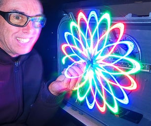
Finally, Insert a 2032 reference battery in its location. Press the button to play the electronic dice.
ENJOY !
(Thanks to IHM3D for the translation)

Grand Prize in the
PCB Design Challenge